Quick Facts
- Material Purity: Required silicon purity reaches 99.999999999% (eleven nines).
- Technological Precision: Extreme ultraviolet lithography uses a 13.5nm light wavelength to etch patterns.
- Manufacturing Complexity: A single chip can involve more than a thousand precisely controlled steps.
- Economic Scale: Worldwide semiconductor revenue reached approximately $655.9 billion in 2024, a 21 percent increase from the previous year.
- Future Roadmap: The industry is moving toward 1.6nm (A16) nodes by 2026 using nanosheet architecture.
- Environment: Fabrication occurs in ISO Class 1 clean rooms, which are thousands of times cleaner than a hospital operating room.
Computer chip manufacturing is the most complex industrial process on Earth. It begins with common sand and ends with billions of transistors etched into silicon. This journey involves transforming quartz into high-purity monocrystalline silicon wafers, which then undergo extreme ultraviolet lithography and complex semiconductor manufacturing steps to create the processors that power everything from your smartphone to massive AI data centers.
From Quartz to Crystal: Refining the Silicon Wafer
If you are a PC builder or a hardware professional, you spend a lot of time looking at the finished product—the polished heat spreader of a CPU or the intricate traces on a motherboard. But the silicon wafer fabrication process starts in a much more humble place: the ground. Specifically, it starts with quartz-rich sand. While sand is essentially silicon dioxide, it is far from being ready for a motherboard.
The first step in computer chip manufacturing is refining this sand into metallurgical-grade silicon. This material is then processed further through a series of chemical reactions to reach a staggering purity level of 99.999999999 percent, often called eleven nines purity. To put that in perspective, if this were a pile of ten billion white marbles, only one single marble could be the wrong color.
Once this purity is achieved, the silicon is melted in a crucible. A tiny seed crystal is dipped into the molten silicon and slowly rotated and pulled upward. This is known as the Czochralski process. It results in a massive, heavy cylinder of monocrystalline silicon called an ingot. This ingot is then sliced with incredible precision using diamond saws into thin discs known as wafers. These wafers are polished until they have a mirror-like finish, ready to serve as the canvas for the world's most advanced circuitry.
Drawing the Circuitry: Extreme Ultraviolet (EUV) Lithography
If the silicon wafer is the canvas, then photolithography is the brush. However, we are no longer using traditional light. As we push toward and beyond the 3nm node, the industry relies on extreme ultraviolet lithography explained as the most critical breakthrough in modern physics.
Traditional deep ultraviolet (DUV) light has a wavelength of 193 nanometers. Trying to etch a 3nm transistor with a 193nm light source is like trying to write a Shakespearean sonnet using a giant whiteboard marker. To get smaller, we need a finer tip. This is where extreme ultraviolet light comes in, sporting a wavelength of just 13.5 nanometers.
The role of extreme ultraviolet light in modern chip fabs is managed almost exclusively by machines from a Dutch company called ASML. These machines are massive, costing upwards of $200 million each. Inside, a high-power laser hits a tiny droplet of molten tin 50,000 times per second. This creates a plasma that emits EUV light. Because EUV light is absorbed by almost everything—including air and glass—the entire process must happen in a vacuum, using a series of ultra-precise mirrors rather than lenses to bounce the light onto the wafer.
This light passes through a mask (a stencil of the circuit design) and hits a light-sensitive coating on the wafer called photoresist. This step-by-step guide to the photolithography process essentially "prints" the blueprint of billions of transistors onto the silicon. As we look toward the 2026 update for hardware, High-NA (Numerical Aperture) EUV machines will become the standard, allowing for even tighter transistor density and keeping Moore's Law on life support for a few more years.
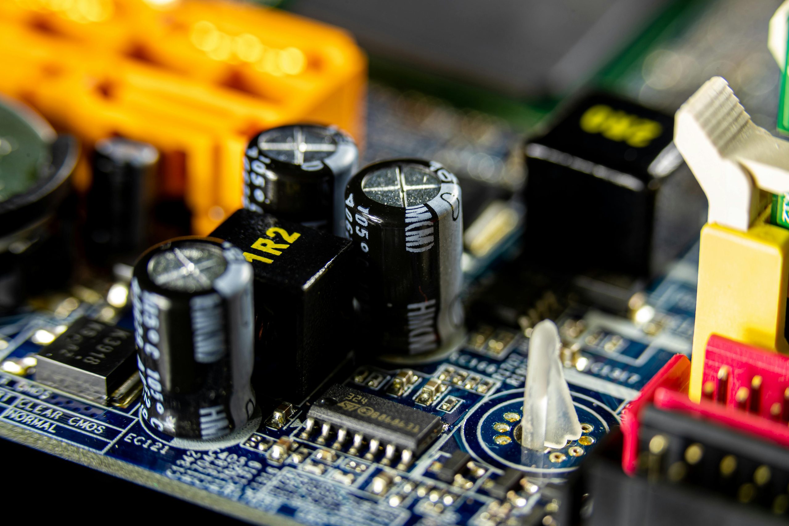
Building the 3D Structure: Deposition, Etching, and GAA
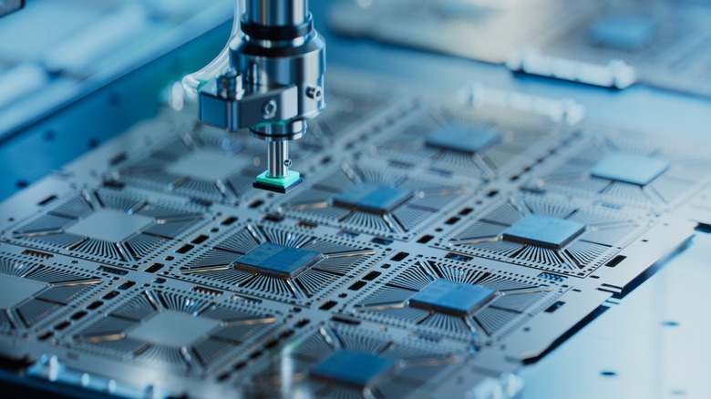
Patterning the wafer with light is just the beginning. After the "drawing" is done, we have to actually build the physical structures. Modern semiconductor manufacturing involves more than a thousand precisely controlled steps to create a single integrated circuit, building the components layer by layer.
This phase involves three primary techniques:
- Deposition: Ultra-thin layers of conducting or insulating materials are grown or sprayed onto the wafer surface.
- Etching: Precise chemicals or gases (plasma etching) remove the unwanted material left behind by the lithography process, leaving only the desired circuit pattern.
- Ion Implantation: Atoms are fired into the silicon to change its electrical properties, creating the "switches" that we know as transistors.
The architecture of these transistors is currently undergoing a massive shift. For years, we used FinFET (Fin Field-Effect Transistor) designs. However, to maintain performance at the sub-3nm level, the industry is transitioning to nanosheet architecture, also known as Gate-All-Around (GAA).
How gate all around transistors improve chip performance is down to control. In a GAA setup, the gate surrounds the channel on all four sides, significantly reducing current leakage and improving power efficiency. Furthermore, manufacturers are introducing technology like backside power delivery. By moving the power wires to the bottom of the silicon slab rather than the top, how backside power delivery reduces chip interference becomes clear: it clears the "traffic jam" of wires on the top layer, allowing for more direct power and better signal integrity for high-performance computing.
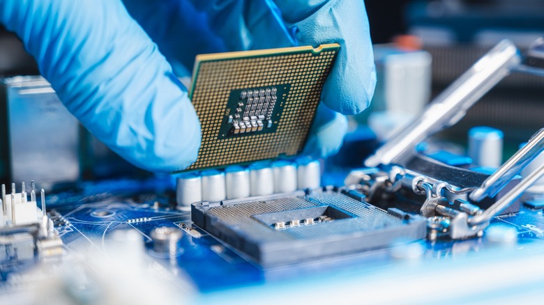
Advanced Packaging: The Rise of CoWoS for AI
In the past, once the chips were cut from the wafer, they were simply placed in a plastic housing and soldered onto a board. Those days are over. For modern AI processors like those from NVIDIA or AMD, the "packaging" is just as complex as the chip manufacturing itself.
This is where the role of cowos in connecting gpus and high bandwidth memory becomes vital. CoWoS, or Chip-on-Wafer-on-Substrate, is a 2.5D and 3D packaging technology. Instead of having a GPU and its memory far apart on a green PCB, CoWoS allows them to be placed on a silicon interposer—essentially a high-speed landing pad. This allows for thousands of tiny connections, providing the massive data throughput required for large language models to function.
Without these advanced packaging techniques, the world’s fastest AI chips would be bottlenecked by how slowly data moves between the processor and the memory. As we move deeper into the decade, we will see more "chiplet" designs where different parts of a CPU are made on different nodes and stitched together into a single high-performance package.
FAQ
How are computer chips made?
The process involves refining sand into 99.999999999% pure silicon, slicing it into wafers, and using extreme ultraviolet lithography to etch billions of transistor patterns. These patterns are then physically built using deposition and etching before being packaged into a finished processor.
What materials are used to make computer chips?
The primary material is silicon, derived from quartz sand. Other essential materials include copper for wiring, various chemicals for photoresist and etching, and rare earth elements for doping the silicon to change its conductivity.
Why is computer chip manufacturing so difficult?
It requires absolute precision at the atomic scale. Even a single speck of dust can ruin a chip, requiring specialized clean rooms. Furthermore, the physics of manipulating 13.5nm light and preventing electrical leakage in transistors only a few atoms wide pushes the limits of human engineering.
What is photolithography in semiconductor manufacturing?
Photolithography is a process that uses light to transfer a geometric pattern from a photo mask to a light-sensitive chemical photoresist on the wafer. It is essentially the printing process that determines where the transistors and wires will be located on the chip.
What are the different stages of chip manufacturing?
The stages are generally categorized into wafer preparation (slicing and polishing), front-end-of-line (lithography and transistor formation), back-end-of-line (creating the metal interconnects), and back-end assembly (testing and packaging).
Why are computer chips so expensive to produce?
The cost is driven by the massive investment required for a semiconductor foundry. A modern fab can cost over $20 billion to build, and the machines used for lithography cost hundreds of millions each. Additionally, the thousands of steps involved in the process and the high cost of maintaining a sterile environment add to the final price tag.